- Project NameMIPS Pipelined CPU Design
- Project Type & Time2020, Course Design
- My dutyComplete independently
- Technology InvolvedVerilog Programming, Hardware Design
- IDEVivado
MIPS Pipelined CPU Design
The course design of Computer Design Practice, got a score of 100%
System Design
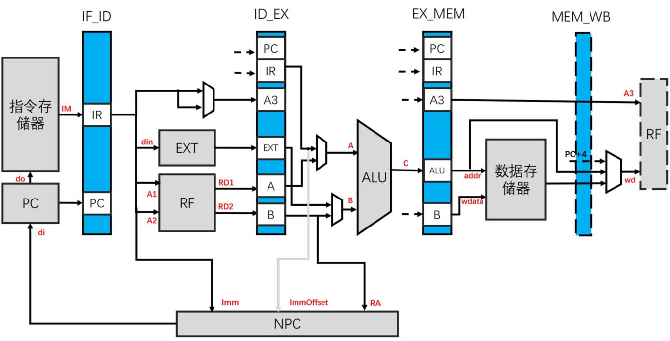
As shown in the figure, the execution process of each instruction is divided into five phases of fetching IF, ID, EX, MEM, and WB. Except for the combination of the WB phase and the rising edge of the clock, the remaining four phases are all combinational logic circuits. , Insert timing modules at the junction of the phases. These modules contain several registers, which will be triggered by the rising edge of the clock, pass the calculation results of the previous phase to the latter phase, and are controlled by signals such as reset, hold, and clear. And the WB stage does not have the necessary combinational logic operation, so the selection of the write-back content and the generation of the write-back control signal are migrated to the MEM stage. At the rising edge of the clock at the end of the MEM stage, the write-back content is directly written into the RF.

In order to make the instructions "flow" in the four stages, PC and IR registers are set at each junction, and the instructions are passed back one by one when the pipeline is working normally so that the instructions executed in each stage at the same time can be guaranteed to be independent. Set up an independent control module in the later stage of the junction to generate control signals according to the IR content of this stage. In addition, according to the requirements of the later stage operation, each junction needs to set a unique register: ID_EX needs to pass the output EXT of the expansion unit and the output of the register file to the EX stage as candidates for the ALU operand; EX_MEM needs to calculate the ALU The result is passed to the later stage, and the contents of the B register of the previous stage are passed to the MEM stage as the write data; and ID_EX, EX_MEM need to set the A3 register, and write the register number determined in the ID stage, all the way from the ID stage Pass to the WB stage.
PC Updating Strategy
In general, the PC only needs to increment by 4 at each rising edge to get the next instruction, but the jump instruction needs to update the PC with a special value. Analyze all jump instructions. Among them, conditional jump instructions such as BNE, BEQ, BGTZ, etc. need to be determined after the EX stage is over to determine whether to update the PC, JR instructions also need to be in the EX stage to get the determined jump target; while JAL, J The instruction can determine the occurrence of the jump action and the jump target in the ID phase.
Therefore, the PC and NPC in the multi-cycle experiment are slightly modified: the PC+4 function of the NPC is cancelled, the jump addresses of different types of instructions are separated to the ports Imm and ImmOffset, and they are connected to the specific phases of the different types of instructions to complete the jump. Corresponding register. When the input terminal PCWr of the PC is not enabled, the PC itself completes the counting action of incrementing 4 on the clock edge; when the PCWr is enabled, the PC is updated with the output value of the NPC.
When the conditional jump instruction is in the EX stage, if it is determined that a jump occurs, PCWr is pulled up, and the new value calculated by NPC is assigned to the PC. Since the jump instruction has entered the EX stage when PCWr is enabled, it is actually The next two instructions in the jump instruction sequence have been read in, and they are located in the IF and ID phases. Therefore, IF_ID and ID_EX need to be notified to intercept these two instructions, that is, to raise their clr signal to pass the next clock edge to ID and The EX instruction is empty; if it is judged that the jump does not occur, the two instructions are valid and do not need to be intercepted. Similarly, when J, JAL, JR and other instructions enter a specific stage, the jump control module will pull up PCWr to update the PC value, and at the same time notify its previous pipeline registers to intercept useless instructions.
Data Conflict Solution
This pipeline design has RAW data conflicts, so a data hazard processing module is introduced. For the case of one instruction apart, the data is passed from the MEM (bypassing); for the adjacent case, if the write-back result of the previous instruction can be determined in the EX stage, then it is directly passed from the EX stage, if the previous instruction is written back If the data cannot be determined in the EX phase, then the IF and ID phases are notified to suspend for one cycle, and the forward command will be forwarded after the previous command enters the MEM.
The data hazard processing module constructs the MEM-ID and EX-ID pathways. When the pre-passing conditions are met, the A and B passed from the ID stage to the next stage will be given by the forward data instead of the RF output. The module output control signal is connected to the hold port of PC and IF_ID, and the clr port of ID_EX. When the IF and ID are required to be suspended, the hold and clr are pulled up, so that the data in the IF and ID phases will not change when the clock edge comes. The instruction enters the EX phase, and the risky instruction enters the MEM phase, thereby passing the write-back data to the ID through the MEM-ID pre-passing path.
Data Paths
Take the execution of one instruction as an example.
The "do" port of the PC transfers the count value to the distributed memory, and the instruction content is directly obtained through combinatorial logic operations and is transferred to the IR input terminal of IF_ID through the IM port of the instruction memory, and the IF phase ends.
When the rising edge of the clock arrives, the instruction is passed to each register in the ID phase at this time. If the instruction is a J/JAL transfer instruction, the address part of the IR will be passed to the imm port of the NPC. After the new address is calculated by the NPC, it will be passed to the di end of the PC to wait for the clock edge to complete the update of the PC; otherwise, the Key field extraction, take the immediate/offset part of IR as din input of EXT, rs part as A1 input of RF, rt part as A2 input, and rt/rd/0x1f as A3 input to get the extended output EXT, RF read output RD1 and RD2, write register serial number A3, complete instruction decoding, ID phase ends. When the rising edge of the clock arrives, the instruction and ID phase arithmetic results are transferred to the EX phase registers. If the instruction is a JR instruction, then the contents of the EX stage B register will be transferred to the RA port of the NPC, and the NPC will transfer the RA content to the di port of the PC and wait for the clock edge to complete the update of the PC; if the instruction is a conditional transfer instruction, it will The offset/immediate part of IR, the PC is passed to the ImmOffset end of the NPC, and the NPC calculates the effective address and passes it to the di end of the PC. If the branch condition is met, the PC is updated at the clock edge; at the same time, the shmt of EXT, A, B, and IR Partly through the selector, connected to the A and B input terminals of the ALU as operation operands, and the operation result is output at the C terminal. The EX phase is over.
When the rising edge of the clock arrives, the instruction and the result of the EX phase operation are passed to the registers of the MEM phase at this time. The result of the ALU operation will be connected to the addr end of the data memory as the memory access address, and the contents of the B register will be connected to the wdata end as the write memory data. The read data of the data memory, after selection with ALU and PC+4, are passed to the wd end of the register group RF as the write-back content, and the content of the A3 register is passed to the A3 end of the RF, waiting for the next rising edge of the clock. Complete write back. The MEM and WB phases are over.
Examination & Evaluation
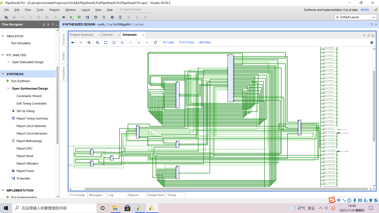
Resource Consumption
This design uses Block Memory as the instruction memory, which consumes fewer resources than Distributed Memory. This project optimizes each combinational logic component, and through the conditional perfection of if and case statements, ensures that no extra latches are generated in each code; the bit width of the PC is reduced to 30 bits, and the IR of the MEM stage is simplified to the best of all It is possible to use fewer signal bits to achieve the same function.
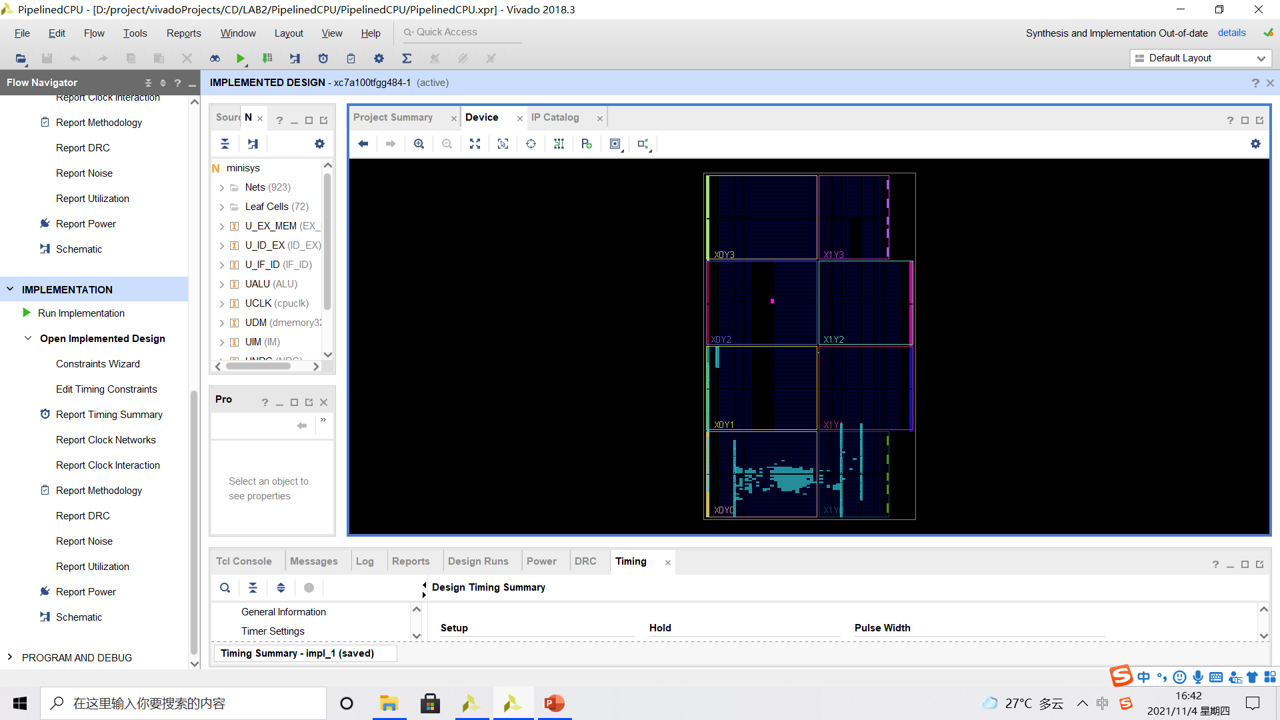
CPU Frequency
Compared with a multi-cycle CPU, the combination delay is increased due to the addition of combinational logic such as forwarding. The highest clock frequency of this five-stage pipeline CPU is lower than the highest clock cycle that a multi-cycle CPU can reach, and the highest clock cycle is 79.4MHz. Through the critical path calculation, the theoretical main frequency is 83.58MHz
On-chip Power
Interpreter Development
I also developed an interpreter that can automatically translate MIPS compiling language into Machine Language(binary codes)
For example, it can transform an compiling language file(.asm):
into a .hex file that can be load into Vivado and executed directly by my CPU: